Compared to mobile phones and tablets, accessory chargers have been less popular, but recently a new technology gallium nitride chargers attracted a wave of heat, gallium nitride chargers with small size and high efficiency features are quickly used by manufacturers.
So what is gallium nitride and what is the difference between gallium nitride chargers and other chargers?

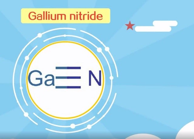
What is gallium nitride?
Gallium nitride (GaN) is a compound of nitrogen and gallium, specific semiconductor characteristics, early application in light-emitting diodes, it and commonly used silicon belong to the same element periodic group, high hardness, high melting point, high stability.
Gallium nitride material is an important semiconductor material for the development of microelectronic devices. It has the characteristics of wide band gap and high thermal conductivity, etc. It can be used in chargers to adapt small transformers and high power devices with high charging efficiency.
The advantages and disadvantages of gallium nitride charger
Advantages: small size, safety
Gallium nitride chargers have the advantages of being smaller, more efficient and safer because of their wider band gap and better thermal conductivity than ordinary semiconductor silicon, and their ability to match smaller transformers and high-power inductors.More recently, flagship phones and tablets have been designed to charge faster, with more powerful chargers, 40W50W chargers being common.More charging power means the charger is getting bigger and hotter.

By switching to gallium nitride technology, the charger can be greatly reduced in size and is very portable. At the same time, the gallium nitride charger can also maintain high efficiency and low temperature operating state, and the safety is better.
Cons: High cost
The main drawback of gallium nitride chargers is their high cost.
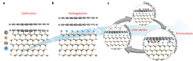
Gallium nitride compounds as a new type of the third generation, synthetic environmental requirement is high, tell from the manufacturing process, no liquid gallium nitride, cannot use traditional draw ferrari the monocrystalline silicon single crystal, pure, was synthesized by gas in the ammonia flow more than half an hour to 1000 – degree heat gallium powder gallium nitride formation, so the cost of gallium nitride charger is higher, corresponding to the gallium nitride charger on market price is higher than the traditional charger a piece.
Application and development of gallium nitride charger
Thanks to the emerging technology in the charging industry, gallium nitride chargers have been embraced by digital manufacturers as soon as they appear. Famous mobile phone brands and third-party accessories manufacturers have started to launch their own gallium nitride chargers. According to R&D, UGreen’s first 65W gallium nitride charger will be released in the near future.
In addition to C-terminal consumer electronics, gallium nitride also has great potential in 5G applications. 5G era requires a lot of micro base stations and intermediaries, which also require more efficient power supply. The advantages of small size and high efficiency of gallium nitride chargers will be obvious.
Gallium nitride application tuyere
The birth of gallium nitride is accompanied by the mission of scientific and technological development to serve the better life of mankind.
Many new technologies, new applications, new markets, gallium nitride from the laboratory to the market moment, is bound to attract global attention.
These emerging markets include 5G, radio frequency, fast charging, and so on. Let’s share with you some of the areas where gallium nitride is currently being commercialized on a large scale.
1. 5G commercialization is approaching
RF gallium nitride technology is a perfect fit for 5G, and base station power amplifiers use gallium nitride.
Gallium nitride (GaN), GaAs (GaAs) and InP (InP) are commonly used in RF applications.
Compared with high-frequency processes such as gallium arsenide and indium phosphide, gallium nitride devices output more power.
Compared with power processes such as LDCMOS and silicon carbide (SiC), GaN has better frequency characteristics.
The higher instantaneous bandwidth of gallium nitride devices is important, and the use of carrier aggregation and the readiness to use higher frequencies of carriers are all in order to achieve greater bandwidth.
Gallium nitride is faster than silicon or other pentavalent devices.
GaN can achieve higher power density.
GaN has the advantage of small size for a given power level.
With smaller devices, the device capacitance can be reduced, making it easier to design higher bandwidth systems.
A key component in the RF circuit is the PA (Power Amplifier).
From the current application, the power amplifier is mainly composed of GaAs power amplifier and complementary metal oxide semiconductor power amplifier (CMOS PA), among which GaAs PA is the mainstream.
But with the arrival of 5G, GaAs devices will not be able to maintain high integration at such high frequencies, so GaN becomes the next hot spot.
As a wide band gap semiconductor, gallium nitride can withstand higher working voltage, which means that its power density and working temperature are higher, so it has the characteristics of high power density, low energy consumption, high frequency and wide band support.
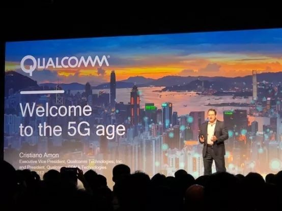
Cristiano Amon, president of Qualcomm, said at the 2018 Qualcomm 4G / 5G Summit that there are expected to be two waves of 5G phones launched in the first half of next year and the end of the Christmas and New Year period, with the first commercial 5G phones coming soon.
5G technology is expected to offer speeds between 10 and 100 times faster than current 4G networks, reaching gigabits per second, while reducing latency more effectively, according to the report.
In multi-input multi-output (MIMO) applications, the key technology of 5 g Massive base station transceiver letters on using large number (such as 32/64) antenna array to achieve a greater wireless data traffic and connection reliability, this architecture need to form a complete set of corresponding rf transceiver cell array, so the number of rf devices will greatly increased, the size of the device is the key, using GaN small size, high efficiency and power density of the characteristics of big can realize high set solutions, such as modular rf front-end device.
At the same time, in 5G millimeter-wave applications, GaN’s high power density characteristics can effectively reduce the number of transmission channels and the size of the overall scheme under the same coverage conditions and user tracking function.
Achieve an optimal combination of performance costs.
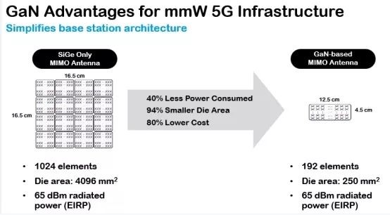
In addition to the base station radio frequency transceiver unit to display the required number of rf devices greatly increases, the density of base station and base station number will also be greatly increased, so compared with 3 g, 4 g era, in the age of 5 g rf devices will increase in the number of dozens of times, even one hundred times, so the cost control is critical, and silicon gallium nitride has great advantage on cost, with the mature of silicon-based gallium nitride technology, it can be to market the breakthrough in the biggest price advantage.
2. Strong demand for fast charging of consumer products
With the increasing size of the screen of electronic products, the power of the charger also increases, especially for high-power fast charging appliances, using the traditional power switch can not change the status quo of the charger.
And GaN technology can do it, because it is the world’s fastest power switching devices, and can in the case of high speed switch still keep high efficiency levels, can be used in smaller components, can be effective when applied to the charger to reduce the product size, such as to the typical 45 w adapter design can use 25 w or a smaller form design.
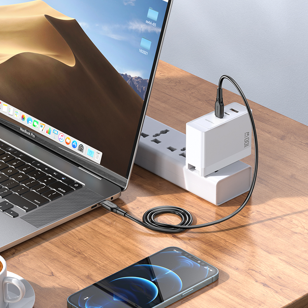
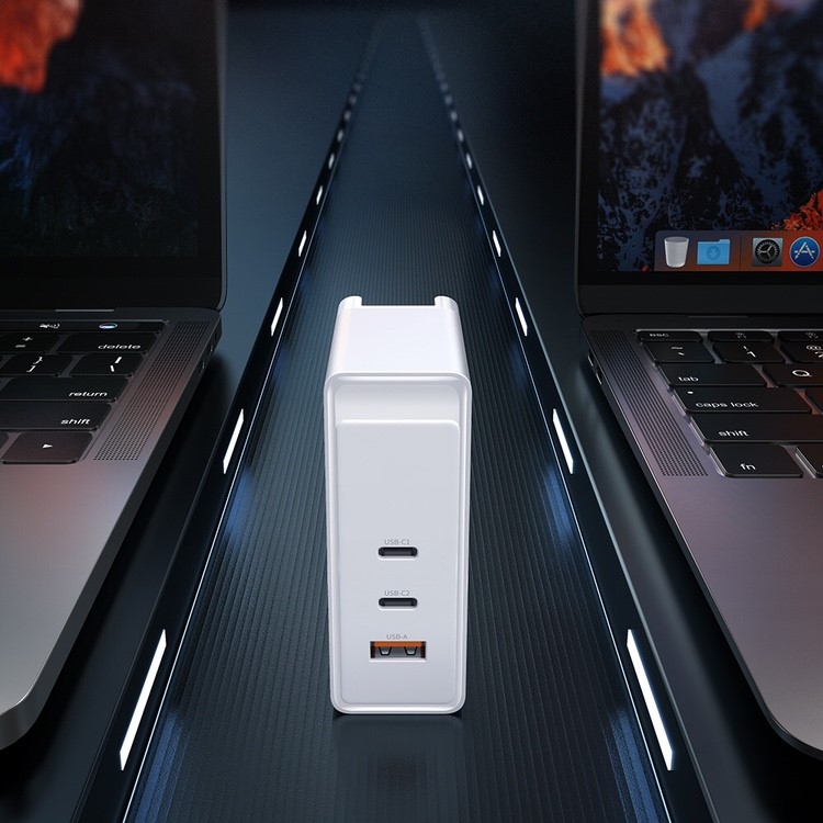
GaN charger has attracted global attention. High speed, high frequency and high efficiency make the high-power USB PD charger no longer a burly brick. Its small size can also achieve high-power output, which is smaller and lighter than Apple’s original 30W charger.
Take a look at the built-in gallium nitride charger side by side with the traditional charger. The output power of the built-in gallium nitride charger is 27W, and the output power of the Apple USB-C charger is 30W. The power difference between the two is not big, but the volume of the built-in gallium nitride charger is completely different.
According to the incomplete statistics of charging head network, as of October 23, 2018, there are 52 mobile phones supporting USB PD fast charging, and another 20 mobile phones supporting USB PD3.0 (PPS) fast charging.
The following is a detailed list of mobile phone models:
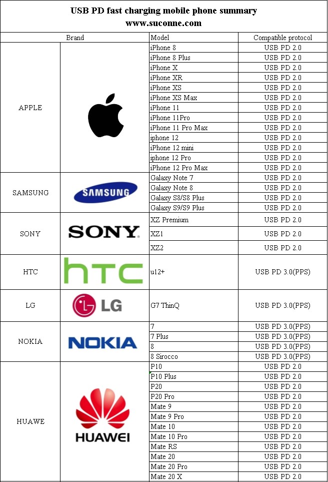
It can be seen that almost all the mainstream mobile phone manufacturers have included USB PD quick charging protocol into the charging configuration of mobile phones.
There are 52 models of USB PD fast charging mobile phones covering 15 brands, including Apple, Huawei, Xiaomi, Samsung and other front-line brands.
From the layout of major mobile phone manufacturers and original chip factories, USB PD fast charging will become the preferred charging scheme for mobile phones, game consoles, notebook computers and other electronic devices at present, while USB Type-C will also become the only interface of power and data transmission between electronic devices in the next decade, and the unification of USB PD fast charging protocol is coming.
3. LiDAR Makes Unmanned Vehicles Safer
Lidar, or LiDAR, uses laser pulses to quickly create three-dimensional images or electronic maps of the environment.
Gallium nitride field effect transistors switch on and off ten times faster than MOSFET devices, giving LiDAR systems advantages such as superior resolution and faster reaction time, and enabling higher accuracy due to superior switching.
These capabilities are driving a new and broader range of LIDAR applications, including applications that detect real-time motion in support of video game applications, gesture-driven computers, and self-driving cars.
In the process of developing and promoting the popularization of automated vehicles, automakers and technology companies are looking for the best combination of sensors and cameras to effectively control costs and maximize the ability to perceive and see the surrounding environment while still being able to produce in large quantities.

Gallium nitride is significantly faster, 100 to 1,000 times faster than silicon in current lidar applications.
This speed means the speed, sharpness and accuracy of the photos taken.
Let’s describe the things ahead of us on the road and the color warning of lane changes.
Lidar can detect the presence of obstacles in the road ahead.
With lidar you can get a much more comprehensive view of terrain changes, terrain that you can’t see.
Neither camera nor radar can do the job, because both have their own shortcomings.
The world’s leading gallium nitride company
In 5G commercial, consumer power fast charging popularization, unmanned driving and other fields, gallium nitride has a broad application space.
As a new third-generation semiconductor technology, gallium nitride is also a market that countries around the world are competing for. At present, many representative forces of gallium nitride have been formed in the market, among which the first echelon includes Innosecco, Nanwei, EPC and other representative enterprises.
Innosecco is currently the world’s first enterprise to adopt 8-inch enhanced gallium nitride epitaxy and chip mass production, and is also a representative of domestic semiconductor enterprises in the first echelon of gallium nitride industry.
1, InnoScience
InnoScience was founded in December 2015. InnoScience is a high-tech enterprise focusing on R&D and industrialization of the third generation semiconductor gallium silicon-based nitride. Currently InnoScience has two R&D and industrialization bases in Zhuhai and Suzhou, China.
Innoseco team has gathered many domestic and foreign elites in the field of gallium nitride. Through continuous innovation, Innoseco has taken the lead in realizing the mass production process of 8-inch gallium nitride based on silicon in the world, and has launched a series of products, and the performance of the products has reached the international leading level.

The secco using IDM complete industrial chain pattern, success in China established a research and development, design, production, testing, sales, marketing, technical support, complete GaN industrial chain, such as improve the GaN wafer manufacturing capacity of the factory, to accelerate the high-performance gallium nitride products into the market, the current leader in China’s third generation of semiconductor manufacturing enterprises.
2.Navitas Micro Semiconductor Inc
Navitas Semiconductor was one of the world’s first GaN power IC companies, founded in 2013 in El Segundo, California.
We have a strong team of power semiconductor industry experts with a strong track record in power electronics.
With more than 200 published patents, the company’s proprietary AllGaN process design suite integrates the highest performance GaN FET with logical and analog circuit monolithic for mobile, consumer,
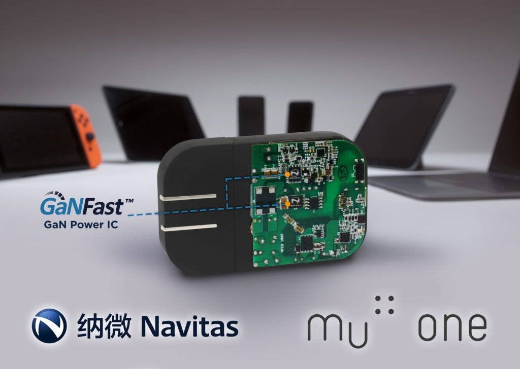
Enterprise and new energy markets provide smaller, more efficient and cheaper power supplies.
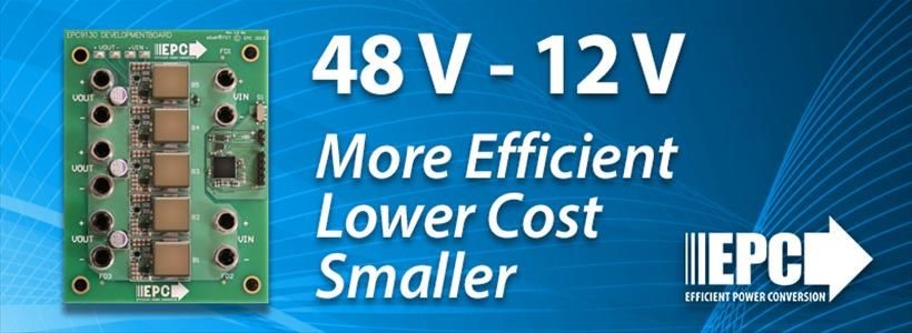
3. EPC IPP power supply
EPC Power Converts (EPC) was founded in November 2007 by three senior engineers with a combined 60 years of experience in advanced power management technologies.
Alex Lidow, CEO of Ip Power Conversion, was the co-inventor of silicon power MOSFET in the 1970s.
In addition to managing R&D and manufacturing positions at International Rectifier Corporation, he served as its Chief Executive Officer for 12 years.
The subsequent evolution of semiconductor technology made it clear to the founders of Ip that silicon technology had reached its limits and the pace at which it could no longer drive innovation and new heights.
Ip Power Conversion was founded on the belief that gallium nitride technology could replace silicon technology in power conversion due to its unrivaled speed, efficiency and low cost.
In fact, gallium nitride technology is an enabling technology with superior crystal properties, which can achieve a performance ratio of 1000:1 compared with silicon technology.
Gallium Nitride Market Prospects
What are the drawbacks of gallium nitride devices?
The downside is that it’s too expensive!
Reviewing the evolution and development of the previous two generations of semiconductor, any generation of semiconductor technology from the laboratory to the market, is faced with the challenge of commercialization.
At present, gallium nitride is also in this stage. With the acceleration of market demand, mass production, technological innovation, etc., the cost of gallium nitride will become civilian, and the final market will replace the traditional silicon-based power devices.
The commercial production of 8-inch silicon-based gallium nitride could significantly reduce the cost.
The popularization of the third generation semiconductor is approaching, and we have the honor to witness the arrival of this moment.